 |
|||
|
Page Title:
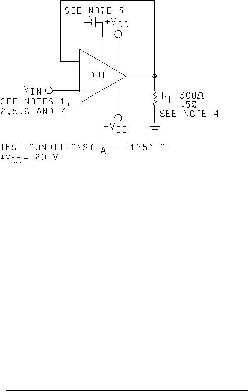
Figure 8. Test circuit, burn-in (steady state power and reverse bias) and operating life test. |
|
||
| ||||||||||
|
|  MIL-M-38510/101H
NOTES:
For device types 02 and 08, VIN = 0.5 V dc, and shall be positive into one amplifier and negative into
1.
the other amplifier.
2.
For device types 01 and 04, VIN = 3.0 V dc. For device type 03, VIN = +3.0 V or 3 V.
3.
A 30 pF compensation capacitor is required for types 03, 04, 05, and 06.
For device types 04 and 06, RL = 1500 Ω. The actual measured value of the resistor selected shall
4.
not exceed 5 percent of its branded value due to use, heat, or age.
For device type 05, VIN = 1.0 V dc, and shall be positive into one amplifier and negative in to the
5.
other amplifier.
6.
For device type 06, VIN = 3.0 V dc, and shall be positive into one amplifier and negative into the
other amplifier.
7.
For device type 07, VIN = 1.0 V dc.
FIGURE 8. Test circuit, burn-in (steady state power and reverse bias) and operating life test.
33
|
|
Privacy Statement - Press Release - Copyright Information. - Contact Us |
