 |
|||
|
Page Title:
Table 1. Electrical performance characteristics-cont. |
|
||
| ||||||||||
|
| 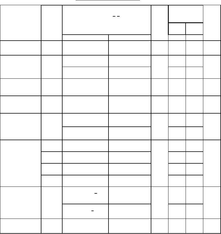 MIL-M-38510/117C
TABLE I. Electrical performance characteristics Continued.
Conditions 1/ 2/
Device
Limits
Unit
Test
Symbol
type
-55C ≤ TA ≤ +125C
see figure 10 and 3.5
Min
Max
unless otherwise specified
Input voltage
Load current
06
-2
2
mV
Thermal regulation
IL = -1.0 A
VIN = 11.25 V,
VRTH
TA = 25C
A
06
-100
-15
Adjust pin current
VIN = 4.25 V
IL = -5 mA
IADJ
-100
-15
VIN = 36.25 V
IL = -5 mA
A
06
-5
5
Adjust pin current
4.25 V ≤ VIN ≤ 36.25 V
ĆIADJ
IL = -5 mA
change versus line
(LINE)
voltage
A
06
-5
5
Adjust pin current
-5.0 A ≤ IL ≤ -5 mA
ĆIADJ
VIN = 6.25 V
change versus
(LOAD)
load current
06
-3.00
-0.05
mA
Minimum load
4.25 V ≤ VIN ≤ 14.25 V,
IQ
current
forced VOUT = 1.4 V
-5.00
-0.2
VIN = 36.25 V forced
VOUT = 1.4 V
06
-16.0
-7.0
A
Output short circuit
VIN = 4.25 V, t = 0.1 ms
IOS1
current
-16.0
-7.0
VIN = 4.25 V, t = 0.5 ms
IOS2
-15.0
-5.0
VIN = 4.25 V, t = 5.0 ms
IOS3
-3.0
-0.20
VIN = 35 V, t = 10 ms
IOS4
Output voltage
06
1.19
1.29
V
RL = 0.25 Ω,
VIN = 4.25 V,
3/
VOUT
recovery after
(RECOV)
CL = 20 F
after IOS3
output short circuit
1.19
1.29
current
RL = 250 Ω
VIN = 35 V,
3/
after IOS4
Voltage start-up
06
1.19
1.29
V
RL = 0.25 Ω,
VIN = 4.25 V
VSTART
CL = 20 F
See footnotes at end of table.
16
|
|
Privacy Statement - Press Release - Copyright Information. - Contact Us |
