 |
|||
|
Page Title:
Table 1. Electrical performance characteristics-cont. |
|
||
| ||||||||||
|
|  MIL-M-38510/11D
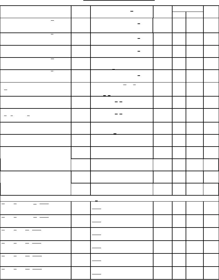
TABLE I. Electrical performance characteristics.
Test
Limits
Conditions 1/
Device
Symbol
type
Unit
Min
Max
A
IIH24
VCC = 5.5 V; VIN = 5.5 V 3/
02
400
High-level input current at G 3 input
A
IIH25
VCC = 5.5 V; VIN = 5.5 V 3/
02
200
High-level input current at P 3 input
A
High-level input current at Cn input
IIH26
VCC = 5.5 V; VIN = 5.5 V 3/
02
160
A
02
700
IIH27
VCC = 5.5 V; VIN = 5.5 V
High-level input current at G 2 input
Cn = 5.5 V 3/
A
IIH28
VCC = 5.5 V; VIN = 5.5 V 3/
02
300
High-level input current at P 2 input
Short-circuit output current at
01
-20
-55
mA
IOS1
VCC = 5.5 V; S3, A 3, B 3 =
G output
5.5 V 3/ 4/
Short-circuit output current at
IOS2
VCC = 5.5 V 3/ 4/
01
-20
-55
mA
Cn+4 output
IOS3
Short-circuit output current at
VCC = 5.5 V 2/ 4/
01
-20
-55
mA
P , F 0 thru F 3 outputs
Short-circuit output current
IOS4
VCC = 5.5 V; VIL = GND;
02
-40
-100
mA
VIN = 5.5 V 4/
A
Collector cutoff current at
ICEX
VCC = 4.5 V; V(A = B) = 5.5 V;
01
250
A = B output
all input = 2.0 V
01
127
mA
Low-level supply current
ICCL1 VCC = 5.5 V; VIL = 0 V;
VIH = 5.5 V
ICCL2 VCC = 5.5 V; VIL = 0 V;
02
65
mA
VIH = 5.5 V
01
135
mA
High-level supply current
ICCH1 VCC = 5.5 V; VIL = 0 V;
VIH = 5.5 V
02
55
mA
ICCH2 VCC = 5.5 V; VIL = 0 V;
VIH = 5.5 V
Propagation delay times, high-to-low level output: 5/
tPHL1
VCC = 5.0 V See figure 4
01
7
46
ns
A I or B I to any F SUM mode
SUM mode test table
01
7
49
ns
VCC = 5.0 V See figure 4
tPHL2
A I or B I to any F DIFF mode
DIFF mode test table
tPHL3
VCC = 5.0 V See figure 4
01
7
40
ns
A I or B I to P SUM mode
SUM mode test table
01
7
40
ns
VCC = 5.0 V See figure 4
tPHL4
A I or B I to P DIFF mode
DIFF mode test table
tPHL5
VCC = 5.0 V See figure 4
01
7
30
ns
A I or B I to G SUM mode
SUM mode test table
01
7
40
ns
VCC = 5.0 V See figure 4
tPHL6
A I or B I to G DIFF mode
DIFF mode test table
See footnotes at end of table I.
6
|
|
Privacy Statement - Press Release - Copyright Information. - Contact Us |