 |
|||
|
Page Title:
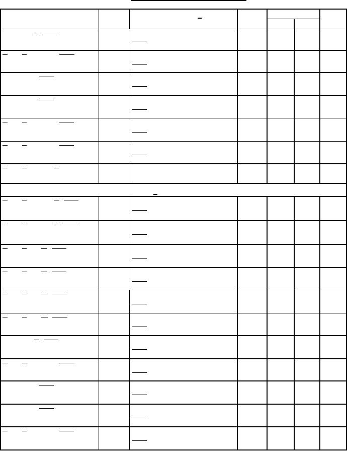
Table 1. Electrical performance characteristics-cont. |
|
||
| ||||||||||
|
|  MIL-M-38510/11D
TABLE I. Electrical performance characteristics.
Limits
Test
Symbol
Conditions 1/
Device
type
Unit
Min
Max
tPHL7
VCC = 5.0 V See figure 4
01
7
25
ns
Cn to any F SUM mode
SUM mode test table
tPHL8
VCC = 5.0 V See figure 4
01
7
76
ns
A I or B I to A = B DIFF mode
DIFF mode test table
tPHL9
VCC = 5.0 V See figure 4
01
7
30
ns
Cn or Cn+4 SUM mode
SUM mode test table
tPHL10
VCC = 5.0 V See figure 4
01
7
30
ns
Cn to Cn+4 DIFF mode
DIFF mode test table
01
7
41
ns
tPHL11
VCC = 5.0 V See figure 4
A I or B I to Cn+4 SUM mode
SUM mode test table
tPHL12
VCC = 5.0 V See figure 4
01
7
50
ns
A I or B I to Cn+4 DIFF mode
DIFF mode test table
tPHL13
VCC = 5.0 V See figure 4
01
7
49
ns
A I or B I to any F logic mode
logic mode test table
Propagation delay times, low-to-high level output: 5/
tPLH1
VCC = 5.0 V See figure 4
01
7
60
ns
A I or B I to any F SUM
SUM mode test table
mode
01
7
69
ns
tPLH2
VCC = 5.0 V See figure 4
A I or B I to any F DIFF
DIFF mode test table
mode
tPLH3
VCC = 5.0 V See figure 4
01
7
27
ns
A I or B I to P SUM mode
SUM mode test table
tPLH4
VCC = 5.0 V See figure 4
01
7
40
ns
A I or B I to P DIFF mode
DIFF mode test table
01
7
27
ns
tPLH5
VCC = 5.0 V See figure 4
A I or B I to G SUM mode
SUM mode test table
VCC = 5.0 V See figure 4
tPLH6
01
7
40
ns
A I or B I to G DIFF mode
DIFF mode test table
01
7
27
ns
tPLH7
VCC = 5.0 V See figure 4
Cn to any F SUM mode
SUM mode test table
tPLH8
VCC = 5.0 V See figure 4
01
7
80
ns
A I or B I to A = B DIFF mode
DIFF mode test table
01
7
28
ns
tPLH9
VCC = 5.0 V See figure 4
Cn to Cn+4 SUM mode
SUM mode test table
01
7
28
ns
tPLH10
VCC = 5.0 V See figure 4
Cn to Cn+4 DIFF mode
DIFF mode test table
01
7
50
ns
VCC = 5.0 V See figure 4
tPLH11
A I or B I to Cn+4 SUM mode
SUM mode test table
See footnotes at end of table I.
7
|
|
Privacy Statement - Press Release - Copyright Information. - Contact Us |