 |
|||
|
Page Title:
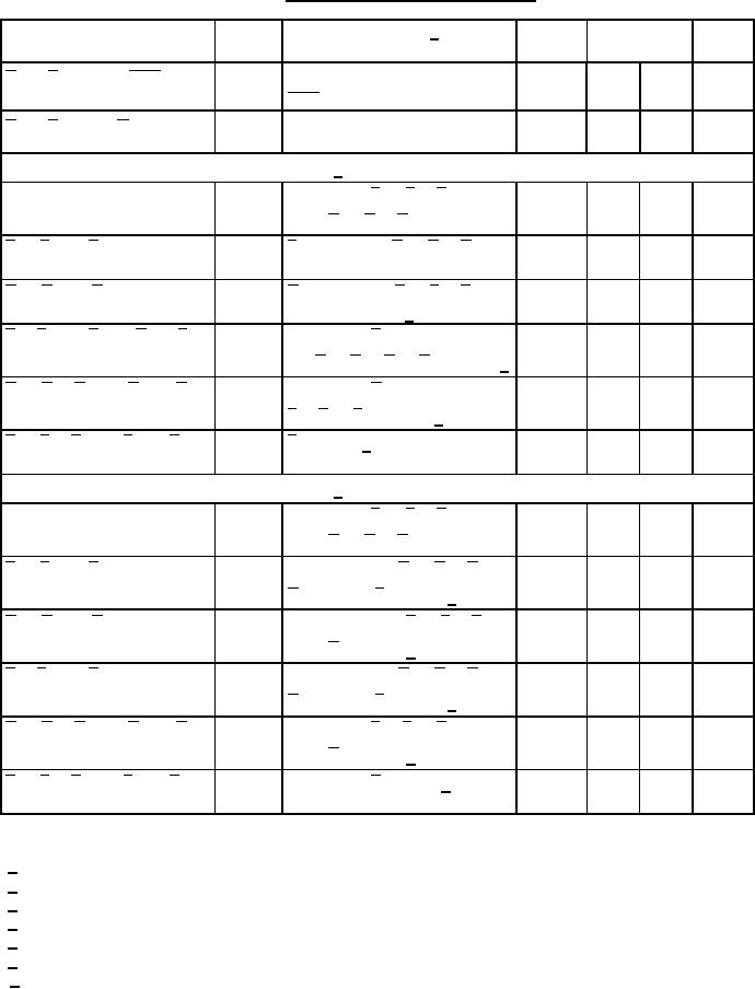
Table 1. Electrical performance characteristics-cont. |
|
||
| ||||||||||
|
|  MIL-M-38510/11D
TABLE I. Electrical performance characteristics.
Test
Symbol
Conditions 1/
Device
Limits
type
Unit
01
7
50
ns
tPLH12
VCC = 5.0 V See figure 4
A I or B I to Cn+4 DIFF mode
DIFF mode test table
tPLH13
VCC = 5.0 V See figure 4
01
7
69
ns
A I or B I to any F logic mode
logic mode test table
Propagation delay times, high-to-low level output: 6/
Cn to Cn+x, Cn+y, Cn+2
tPHL1
02
6
35
ns
VCC = 5.0 V; P 0 , P 1 , P 2 =
GND; G 0 , G 1, G 2 = 2.4 V
tPHL2
02
3
32
ns
P 0 , P 1 , or P 2 to Cn+x,
P I = GND; Cn, G 0 , G 1, G 2 =
Cn+y, Cn+z
VCC = 5.0 V
02
3
32
ns
tPHL3
G 0 , G 1, or G 2 to Cn+y,
G I = 2.4 V; Cn, P 0 , P 1 , P 2 =
Cn+x, Cn+z
GND, VCC = 5.0 V 7/
02
3
35
ns
tPHL4
P 1 , P 2 , or P 3 to G or P
VCC = 5.0 V; P I = GND;
Cn, G 0 , G 1, G 2 , G 3 = 2.4 V 7/
tPHL5
02
3
35
ns
G 0 , G 1, G 2 , or G 3 to G
VCC = 5.0 V; G I = 2.4 V;
P 1 , P 2 , P 3 = GND 7/
tPHL6
02
3
35
ns
P 0 , P 1 , P 2 , or P 3 to P
P I = GND 7/
Propagation delay times, low-to-high level output: 6/
Cn to Cn+x, Cn+y, Cn+2
tPLH1
02
6
29
ns
VCC = 5.0 V; P 0 , P 1 , P 2 =
GND; G 0 , G 1, G 2 = 2.4 V
02
3
25
ns
tPLH2
P 0 , P 1 , or P 2 to Cn+x,
VCC = 5.0 V; Cn, G 0 , G 1, G 2 ,
Cn+y, Cn+z
G 3 = 2.4 V; PI = GND 7/
tPLH3
02
3
25
ns
G 0 , G 1, or G 2 to Cn+y,
VCC = 5.0 V; Cn, P 0 , P 1 , P 2 =
Cn+x, Cn+z
GND; G I = 2.4 V 7/
02
3
26
ns
tPLH4
P 1 , P 2 , or P 3 to G or P
VCC = 5.0 V; Cn, G 0 , G 1, G 2 ,
G 3 = 2.4 V; PI = GND 7/
02
3
26
ns
tPLH5
G 0 , G 1, G 2 , or G 3 to G
VCC = 5.0 V; P 1 , P 2 , P 3 =
GND; G I = 2.4 V 7/
tPLH6
02
3
26
ns
P 0 , P 1 , P 2 , or P 3 to P
VCC = 5.0 V; P I = GND 7/
NOTES:
1/ Condition of inputs specified in table III.
2/ All unspecified inputs at 5.5 V.
3/ All unspecified inputs at 0 V.
4/ Not more than one output should be shorted at a time.
5/ In AI and BI, I = 0, 1, 2, 3.
6/ In GI and PI, I = 0, 1, 2, or 3.
7/ If not under test.
8
|
|
Privacy Statement - Press Release - Copyright Information. - Contact Us |