 |
|||
|
Page Title:
Table 1. Electrical performance characteristics. |
|
||
| ||||||||||
|
| 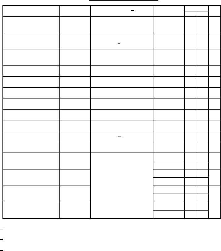 MIL-M-38510/203E
TABLE I. Electrical performance characteristics.
Characteristic
Symbol
Conditions 1/
Limits
Device
Unit
-55C ≤ TC ≤ +125C
type
Min Max
High level output voltage
VOH
VCC = 4.5 V;
02,04
2.4 ---
V
IOH = -2 mA,
VIL = 0.8 V, VIH = 2.0 V
Low level output voltage
VOL
VCC = 4.5 V;
01,02
---
0.5
V
IOL = 16 mA 2/
03,04
VIL = 0.8 V, VIH = 2.0 V
Input clamp voltage
VIC
VCC = 4.5 V;
01,02
---
-1.5
V
IIN = -10 mA;
03,04
TC = 25C
μA
Maximum collector cut-off
ICEX
VCC = 5.5 V;
01,03
---
100
current
VO = 5.2 V
μA
High impedance (off-state)
IOHZ
VCC = 5.5 V;
02,04
---
100
output high current
VO = 5.2 V
μA
High impedance (off-state)
IOLZ
VCC = 5.5 V;
02,04
---
-100
output low current
VO = .5 V
μA
High level input current
IIH1
VCC = 5.5 V;
01,02
---
50
VIN = 5.5 V
03,04
μA
High level input current
IIH2
VCC = 5.5 V; VIN = 4.5 V;
01,02
---
100
special program pin
03,04
μA
Low level input current
IIL
VCC = 5.5 V;
01,02
-1
-250
VIN = 0.5 V
03,04
Short circuit output
IOS
VCC = 5.5 V; 3/
02,04
-10 -100 mA
current
VO = 0.0 V
Supply current
ICC
VCC = 5.5 V;
01,02
---
130
mA
VIN = 0; outputs open
03,04
Propagation delay time
tPHL1
VCC = 4.5 V and 5.5 V;
01, 02
---
75
ns
high-to-low level logic,
CL = 30 pF minimum;
03, 04
---
35
address to output
see figure 5
Propagation delay time
tPLH1
01, 02
---
75
ns
low-to-high level logic,
03, 04
---
35
address to output
Propagation delay time
tPHL2
01, 02
---
35
ns
high-to-low level logic,
03, 04
---
20
enable to output
ns
Propagation delay time
tPLH2
01, 02
---
35
low-to-high level logic,
03, 04
---
20
enable to output
1/ Complete terminal conditions shall be specified in table III.
2/ IOL = 12 mA for circuit B.
3/ Not more than one output shall be grounded at one time. Output shall be at high logic level prior
to test.
4
|
|
Privacy Statement - Press Release - Copyright Information. - Contact Us |
