 |
|||
|
Page Title:
Table 3. Group A inspection for device type 02, 04-cont. |
|
||
| ||||||||||
|
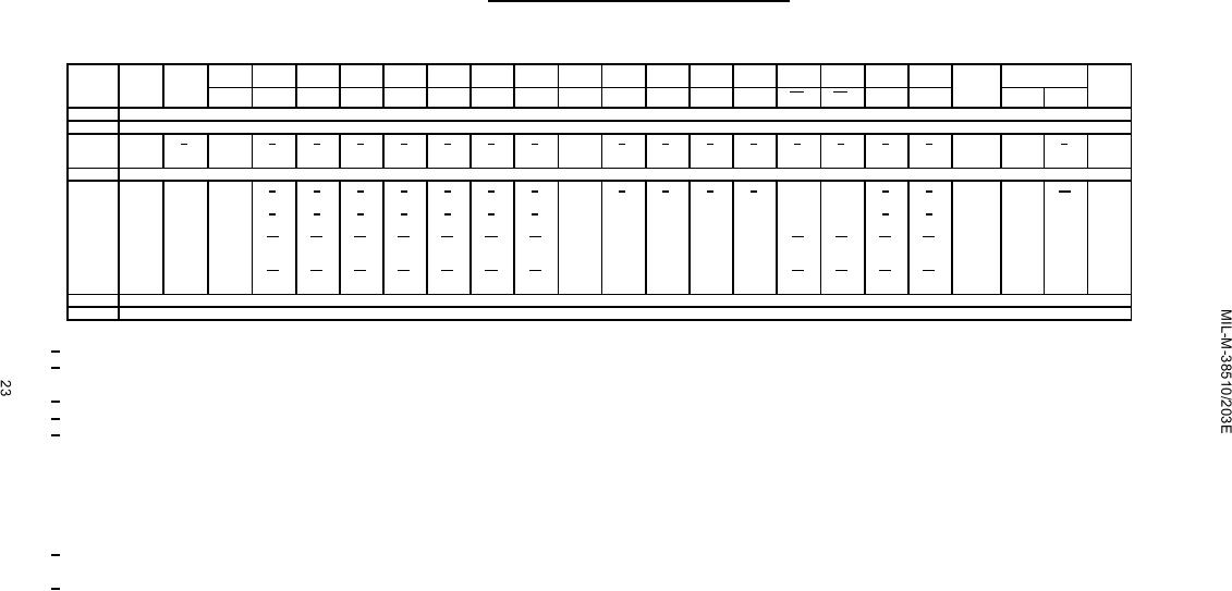
|  TABLE III. Group A inspection for device type 02, 04.
Terminal conditions Outputs: Not designated are open or resistive coupled to GND or voltage
.
Inputs: Not designated are high ≥ 2.0 V, low ≤ 0.8 V, or open.
Subgroup
Symbol
MIL-
Cases
1
2
3
4
5
6
7
8
9
10
11
12
13
14
15
16
Measured
Test limits
Unit
STD-883
E,F
terminal
method Test no.
A6
A5
A4
A3
A0
A1
A2
GND
O4
O3
O2
O1
A7
VCC
Min
Max
CE
CE
1
2
Same tests, terminal conditions, and limits as for subgroup 1, except TC = +125C and VIC tests are omitted.
2
Same tests, terminal conditions, and limits as for subgroup 1, except TC = -55C and VIC tests are omitted.
3
Funct-
5/
7
52
5/
5/
5/
5/
5/
5/
5/
GND
5/
5/
5/
5/
5/
5/
5/
5/
Outputs
5/
TC=+25C
ional
test
Same tests, terminal conditions, and limits as for subgroup 7, except TC = +125C and -55C.
8
9
tPHL1
GALPAT
53
8/
8/
8/
8/
8/
8/
8/
GND
9/
9/
9/
9/
GND
GND
8/
8/
Outputs
11/
ns
TC=+25C
Fig. 4
GALPAT
54
8/
8/
8/
8/
8/
8/
8/
"
GND
8/
8/
"
tPLH1
"
"
"
"
GND
"
"
Fig. 4
tPHL2
Sequen-
55
10/
10/
10/
10/
10/
10/
10/
"
"
"
"
"
10/
10/
10/
10/
"
"
"
tial
Fig. 4
Sequen-
56
10/
10/
10/
10/
10/
10/
10/
"
10/
10/
10/
10/
"
tPLH2
"
"
"
"
"
"
tial
Fig. 4
Same tests, terminal conditions, and limits as subgroup 9, except TC = +125C.
10
Same tests, terminal conditions, and limits as subgroup 9, except TC = -55C.
11
1/ For programmed devices, select an appropriate address to acquire the desired output state, VIL = 0.8 V, VIH = 2.0 V.
2/ 16 mA for circuits A, C and G.
12 mA for circuit B.
3/ For unprogrammed devices, apply 12.0 V on pin 6 (A1) for circuit B devices.
4/ For unprogrammed devices, apply 13 V on pins 1 (A6) and 2 (A5) for circuit A devices.
5/ The functional tests shall verify that no fuses are blown for unprogrammed devices or that the truth table specified in the altered item drawing exists for
programmed devices (see 3.3.2). All bits shall be tested. Terminal conditions shall be as follows:
a. Inputs: H = 3.0 V, L = GND
b. Outputs: Output voltage shall be either:
1. H = 2.4 V minimum and L = 0.5 V maximum when using a high speed checker double comparator, or
2. H ≥ 1.0 V and L ≤ 1.0 V when using a high speed checker single comparator.
c. The functional tests shall be performed with VCC = 4.5 V and VCC = 5.5 V.
6/ For unprogrammed 02 devices (82S129); apply 10.0 V on pin 15 (A7), apply 0.5 V on pin 2 (A5) and 5.0 V on all other address lines for circuit C devices. For
unprogrammed 04 devices (82S129A) apply 10.0 V on pin 5 (A0) and 5.0 V on all other address pins for the circuit C devices.
7/ 2.4 V for circuit B devices.
|
|
Privacy Statement - Press Release - Copyright Information. - Contact Us |