 |
|||
|
Page Title:
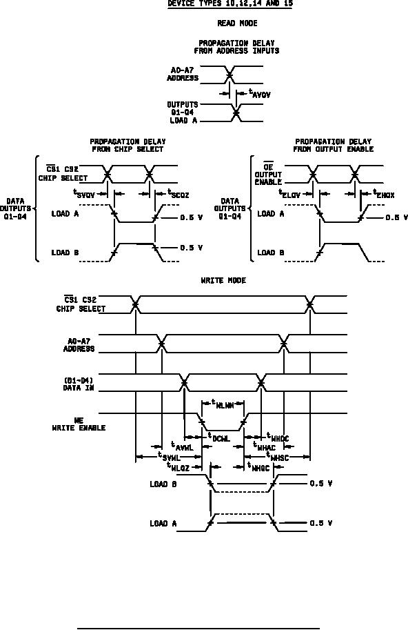
Figure 5. Switching time load circuits, test conditions and waveforms Device types 10, 12, 14, and 15 |
|
||
| ||||||||||
|
|  MIL-M-38510/231C
(All above measurements referenced to 1.5 V unless otherwise indicated)
NOTE:
Timing Diagram represents one solution which results in an optimum cycle time. Timing may be
changed to fit various applications as long as the worst case limits are not violated.
FIGURE 5. Switching time load circuits, test conditions and waveforms Continued.
20
|
|
Privacy Statement - Press Release - Copyright Information. - Contact Us |