 |
|||
|
Page Title:
Table 1. Electrical performance characteristics. |
|
||
| ||||||||||
|
| 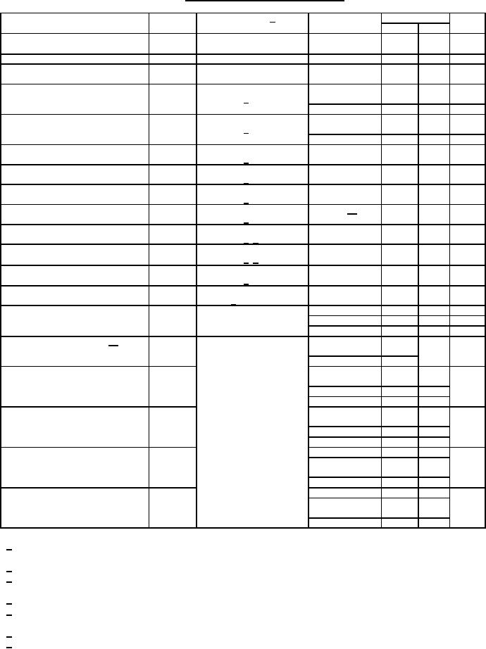 MIL-M-38510/2G
TABLE I. Electrical performance characteristics.
Test
Symbol
Conditions 9/
Device
Limits
Units
Type
Min
Max
All
2.4
--
Volts
High-level output voltage
VOH
VCC=4.5 V
IOH = -400 A
Low-level output voltage
VOL
VCC = 4.5 V, IOL=16 mA
All
0.4
Volts
All
-1.5
Volts
Input clamp voltage
VIC
VCC = 4.5 V, IIC = -12 mA
TC = 25C
Low-level input current
IIL1
VCC = 5.5 V
01, 02, 03, 04,
-0.7
-1.6
mA
VIN = 0.4 V 1/
05, 06
07
-0.5
-1.6
mA
Low-level input current
IIL2
VCC = 5.5 V
01, 02, 03, 04,
-1.4
-3.2
mA
VIN = 0.4 V 2/
05
07
-1.0
-3.2
mA
01, 02, 03, 04
-0.7
-3.2
mA
Low-level input current
IIL3
VCC = 5.5 V
VIN = 0.4 V 6/
A
All
40
High-level input current
IIH1
VCC = 5.5 V
VIN = 2.4 V 5/
A
All
100
High-level input current
IIH2
VCC = 5.5 V
VIN = 5.5 V 5/
A
All 11/
High-level input current
IIH3
VCC = 5.5 V
80
VIN = 2.4 V 3/
A
All
200
High-level input current
IIH4
VCC = 5.5 V
VIN = 5.5 V 3/ 7/
A
01, 02, 03, 04,
-50
-850
High-level input current
IIH5
VCC = 5.5 V
VIN = 2.4 V 7/ 8/
05, 07
120
A
A
05, 07
300
High-level input current
IIH6
VCC = 5.5 V
VIN = 5.5 V 8/
All
-20
-57
mA
Short-circuit output current
IOS
VCC = 5.5 V
VIN = 0 4/
Supply current per device
ICC
VCC = 5.5 V
01
20
mA
VIN = 5 V
02, 03, 04
40
05, 06, 07
30
Maximum clock frequency 10/
fMAX
01, 02, 03
10
MHz
04, 05, 07
06
15
Propagation delay to high logic level
tPLH
01, 02, 03, 04,
5
39
ns
(clear or preset to output)
05
06
5
62
07
5
31
VCC = 5 V
Propagation delay to low logic level
tPHL
01, 02, 03, 04,
5
50
ns
CL = 50 pF minimum
(clear or preset to output)
05
RL = 390Ω 5%
06
5
62
07
5
39
Propagation delay to high logic level
tPLH
06
5
62
ns
(clock to output)
01, 02, 03, 04,
5
39
05
07
5
31
Propagation delay to low logic level
tPHL
06
5
62
ns
(clock to output)
01, 02, 03, 04,
5
50
05
07
5
39
1/ Input condition J or K for device types 01, 02, 03, 04, 06, and preset or D for device types 05 and 07, and
clock, clear or preset for device type 06.
2/ Input condition Clock for device types 01, 02, 03 and 04, and clear or clock for device types 05 and 07.
3/ Input condition Clear or preset for device types 01, 02, 03, 04, 05, 06 and 07 and clock for device types 05
and 07.
4/ No more than one output should be shorted at a time.
5/ Input condition J or K for device types 01, 02, 03, 04, 06, and D for device types 05 and 07, and clock for
device type 06.
6/ Input condition Clear or preset for device types 01, 02, 03 and 04.
7/ Input condition Clock for device types 01, 02, 03 and 04.
4
|
|
Privacy Statement - Press Release - Copyright Information. - Contact Us |
