 |
|||
|
Page Title:
Table 3. Group A inspection for device type 03-cont. |
|
||
| ||||||||||
|
| 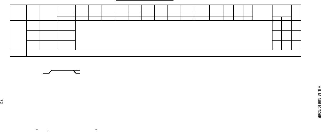 TABLE III. Group A inspection for device type 03 - Continued.
Terminal conditions (pins not designated may be high ≥ 2.0 V or low ≤ 0.7 V or open).
Cases
1
2
3
4
5
6
7
8
9
10
11
12
13
14
Measured
Limits
Unit
MIL-STD-
A,B,C,D
terminal
Subgroup
Symbol
883
Cases 2, X
2
3
4
6
8
9
10
12
13
14
16
18
19
20
method
Test no.
Serial
AIN
BIN
CIN
DIN
Mode
GND
CLK2
CLK1
QD
QC
QB
QA
VCC
Min
Max
10
fMAX
3003
101 to 105
20
---
MHz
Tc = 25C See F,J
(Fig. 6)
106 to 113 Same tests and terminal conditions as for subgroup 9.
3003
5
48
ns
tPLH1
(Fig. 6)
3003
114 to 121
5
56
ns
tPHL1
(Fig. 6)
Same tests, terminal conditions as subgroup 10 except TC = -55C.
11
Notes:
A. Apply input pulse:
2.5 V minimum/5.5 V maximum
0V
B. VIN = 2.5 V.
C. VIN = 0.4 V.
D. Tests numbers 48 through 79 shall be run in sequence.
E. Output voltages shall be either: (1) H ≥2.5 minimum and L ≤0.4 V maximum when using a high speed
checker double comparator; (2) H ≥1.5 V and L ≤1.5 V when using a high speed checker single
comparator.
F. fMAX minimum limit specified is the frequency of the clock input pulse.
The output frequency shall be one-half of the input clock frequency. The input frequency on the
serial input shall be one-half of the clock input frequency and the input shall be shifted such that
are coincident with the clock . Rise and fall times ≤ 6 ns. Input peak
the input
and
voltage 3 to 5 volts.
G. 3.0 V minimum/5.0 V maximum.
J. At the manufacturer's option, the following alternate procedures may be used to guarantee fMAX:
a. Parallel mode. fMAX for the parallel mode shall be guaranteed by performing propagation
delay measurements with the clock pulse width at 1/2 x 1/fMAX. In addition to the
constraints on the clock pulse, the inputs are set to the worst-case condition for the
tset-up and thold requirements. Both positive and negative clock pulse widths shall be
tested. The five tests to justify each JAN fMAX requirement shall be used to test all
possible input/output combinations. A failing limit or nontoggle will indicate that the device
fails to function at fMAX and/or the propagation delay from input to output has exceeded the
allowed limit .
b. Serial mode. fMAX for the serial mode shall be guaranteed by clocking the device four times
(after reset) at fMAX and looking for the QD output to toggle within three periods (3 x
1/fMAX) plus allowed propagation delay. Two tests are performed, depending on the state of
data input, to guarantee both LH and HL transition of the output pulse.
|
|
Privacy Statement - Press Release - Copyright Information. - Contact Us |
