 |
|||
|
Page Title:
Figure 4. Waveforms for propagation delay time and test circuit for device type 01-cont. |
|
||
| ||||||||||
|
| 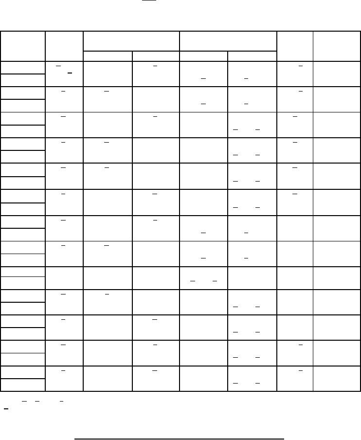 MIL-M-38510/308B
DIFF MODE TEST TABLE
FUNCTION INPUTS: S1 = S2 = 4.5 V, S0 = S3 = M = 0 V
TEST
INPUT
OTHER INPUT
OTHER DATA INPUTS
OUTPUT
OUTPUT
UNDER
SAME BIT
UNDER
WAVEFORM
TEST
APPLY 4.5 V
APPLY GND
APPLY 4.5 V
APPLY GND
TEST
None
Remaining
Remaining
1
tPLH2
A i 1/
Bi
Any F i
tPHL2
B , Cn
A
None
Remaining
Remaining
2
tPLH2
Bi
Ai
Any F i
tPHL2
B , Cn
A
None
None
Remaining
1
tPLH4
Ai
Bi
P
tPHL4
A and B , Cn
None
None
Remaining
2
tPLH4
Bi
Ai
P
tPHL4
A and B , Cn
None
None
Remaining
1
tPLH6
Ai
BI
G
tPHL6
A and B , Cn
None
None
Remaining
tPLH6
2
Bi
Ai
G
tPHL6
A and B , Cn
None
Remaining
Remaining
A=B
1
tPLH8
Ai
Bi
tPHL8
B , Cn
A
None
Remaining
Remaining
A=B
2
tPLH8
BI
Ai
tPHL8
B , Cn
A
tPLH10
Cn
None
None
All
None
Cn+4
1
tPHL10
A and B
None
None
Remaining
Cn+4
2
tPLH12
Ai
Bi
tPHL12
A and B , Cn
None
None
Remaining
Cn+4
1
tPLH12
Bi
Ai
tPHL12
A and B , Cn
None
None
Remaining
1
tPLH13
Ai
Bi
Any F i
tPHL13
A and B , Cn
None
None
Remaining
2
tPLH13
Bi
Ai
Any F i
tPHL13
A and B , Cn
1/ In A i, B i, and F i i = 0, 1, 2, 3.
FIGURE 4. Waveforms for propagation delay time and test circuit for device type 01 - Continued.
14
|
|
Privacy Statement - Press Release - Copyright Information. - Contact Us |
