 |
|||
|
Page Title:
Figure 3. CLEAR switching test circuit and waveforms (device type 07) |
|
||
| ||||||||||
|
| 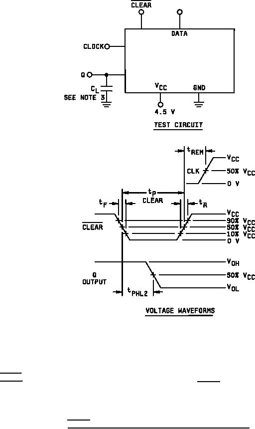 MIL-M-38510/653B
NOTES:
1.
CLEAR pulses are active low and dominate regardless of the state of the clock and data inputs.
CLEAR input pulse characteristics are as follows: tr = tf ≤ 6 ns; tp (CLEAR) ≤ 24 ns; tREM ≤ 30 ns.
2.
CL = 50 pF 10 % (including test jig and probe capacitance).
3.
4.
Clock pulse prior to test with inputs biased to place the output at the appropriate level for test.
5.
Voltage measurements are to be made with respect to the network ground terminal.
FIGURE 3. CLEAR switching test circuit and waveforms (device type 07) - Continued.
31
|
|
Privacy Statement - Press Release - Copyright Information. - Contact Us |
