 |
|||
|
Page Title:
Figure 3. Synchronous switching test circuit and waveforms (device type 08) |
|
||
| ||||||||||
|
| 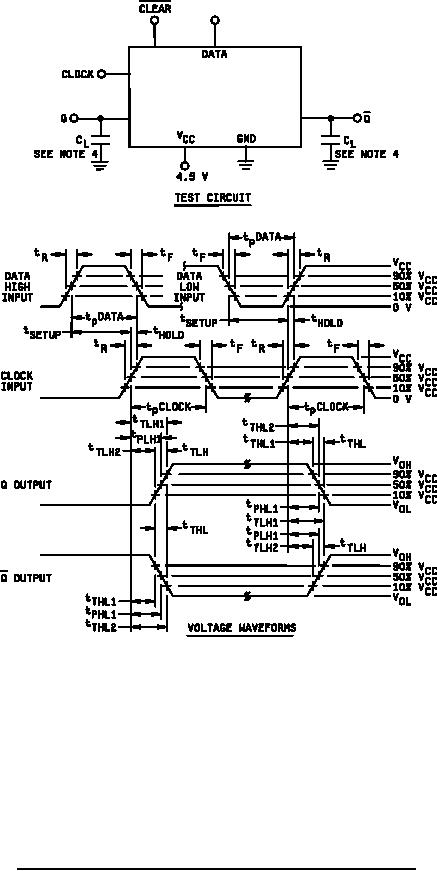 MIL-M-38510/653B
NOTES:
1. Clock input pulse characteristics: tr = tf ≤ 6 ns; tp (clock) ≤ 24 ns.
2. Data input pulse characteristics: tr = tf ≤ 6 ns; tp (data) ≤ 38 ns; tsetup ≤ 30 ns; thold ≤ 8 ns.
3. The clock input characteristics for fMAX are as follows: tr = tf ≤ 6 ns; tp (clock) ≤ 19 ns; PRR ≥ 26 MHz.
4. CL = 50 pF 10 % (including test jig and probe capacitance).
5. Voltage measurements are to be made with respect to network ground terminal.
6. tTLH = tTLH1 tTLH2 ; tTHL = tTHL2 - tTHL1.
FIGURE 3. Synchronous switching test circuit and waveforms (device type 08) - Continued.
32
|
|
Privacy Statement - Press Release - Copyright Information. - Contact Us |
