 |
|||
|
Page Title:
Figure 2. Truth tables and timing diagrams device type 06 |
|
||
| ||||||||||
|
| 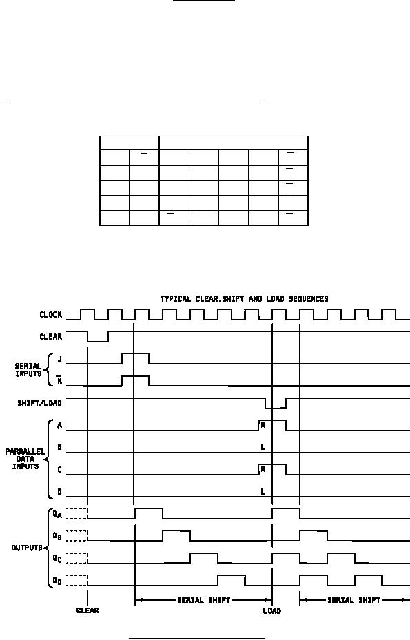 MIL-M-38510/9E
Device type 06
Positive logic:
The registers have two modes of operation:
Parallel (broadside) load
Shift (in direction QA toward QD)
Parallel loading is accomplished by applying the four bits of data and taking the shift/load control input low. The data
is loaded into the associated flip-flop and appears at the outputs after the positive transition of the clock input. During
loading, serial data flow is inhibited.
Shifting is accomplished synchronously when the shift/load control input is high. Serial data for this mode is entered
at the J - K inputs. These inputs permit the first stage to perform as a J - K , D-, or T-type flip-flop as shown in the
truth table.
TRUTH TABLE
Outputs at tn + 1
Inputs at tn
QA
QB
QC
QD
J
QD
K
L
H
QAn
QBn
QCn
QAn
QCn
L
L
QBn
QCn
QAn
L
QCn
H
H
QBn
QCn
QAn
H
QCn
H
L
QAn QBn QCn
QAn
QCn
H = high level, L = low level
NOTES:
1. tn = bit time before clock pulse
2. tn + 1 = bit time after clock pulse
3. QAn = state of QAn at tn.
Figure 2. Truth tables and timing diagrams Continued.
21
|
|
Privacy Statement - Press Release - Copyright Information. - Contact Us |
