 |
|||
|
|
|||
| ||||||||||
|
|  MIL-M-63321A(AR)
4.5.8 Input current (Pins 9, 10, 11). Measure the current into each
pin (9, 10, 11) when it is connected to
Any device failing to
meet the applicable requirement shall be classed defective. This is a
non-destructive test.
4.5.9 Output low. When the output at pins (1, 12, 14, and 15) are
sinking current and held at 1.0 volt, measure the current into each pin.
Any device failing to meet the applicable requirement shall be classed
defective. This is a non-destructive test.
4.5.10 Output high. When the output at pins (1, 12, 14, and 15) are
sourcing current and held at 4.0 voltS, measure the current out of each
pin. Any device failing to meet the applicable requirement shall be
classed defective. This is a non-destructive test.
4.5.11 Switching point. With pin 8 connected to ground and pin 16
connected to 7.5 - 0.1 volts apply 2.5 - 0.10 volts to pin 13, then
confirm that the output voltage at pin 12 is less that 1.5 volts. Apply
5.0 + 0.1 volts to pin 13 and confirm that the output voltage at pin 12
is greater than 6.0 volts. Any device failing to meet the applicable
requirement shall be classed defective. This is a non-destructive test.
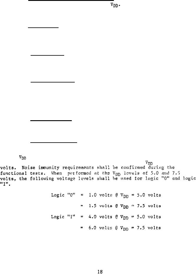
4.5.12 Noise immunity. Noise immunity at input pins (2, 3, 4, 5, 6,
7, 9, 10, 11) shall be confirmed during the functional tests (See
4.5.13). This is a non-destructive test.
4.5.13 Functional tests. The functional tests are to be performed
in a manner that confirms the functional timing diagrams defined in
Figures 1 thru 5. The tests established for figure 1 shall be performed
levels of 5.0 and 7.5 volts, and unless otherwise specified,
at the
level of 5.0
all other functional tests are to be performed at the
Any device failing to meet the applicable requirement shall be classed
defective. This is a non-destructive test.
|
|
Privacy Statement - Press Release - Copyright Information. - Contact Us |