 |
|||
|
|
|||
| ||||||||||
|
|  MIL-T-81290(WP)
0.200 plus or minus 0.001 volts DC! between pins E (+) and
d.
T (-).
e. 28 plus or minus 3 volts DC between pins c (+) and T (-).
3.3.11.2 DMma Output. Elapsed time from the instant the 2.500 voltage
is applied in (c) below until the voltage across pins G (+) and W (-) reaches
4.O plus or minus 0.5 volts DC, shall be as shown in Table 5 after the
application of voltages in the sequence specified in steps (a.) through (c.)
below. The variation of plus voltage between pins G (+) and W (-) shall not
exceed 0.500 volts peak after application of the 100 millisecond pulse in
step (c.) and prior to completion of the time periods specified in Table 5.
a. 10.000 plus or minus 0.010 volts DC to pins W (-) and F (+)
of P3 for not less than 2 seconds.
b. Set-in voltages across pins F (+) and W (-) as specified in
Table 5 for 100 plus or minus 0.1 milliseconds. Rise time of the 100 milli-
second pulse shall not be greater than 150 microseconds and fall time not
greater than 250 microseconds. Pulse width shall be the width measured at
the -25 volt level with a -50 volt set-in. Switching time from presaturation
to set-in voltage shall not be greater than 1 millisecond.
c.
2.500 plus or minus 0.010 volts DC across pins F (+) and W (-).
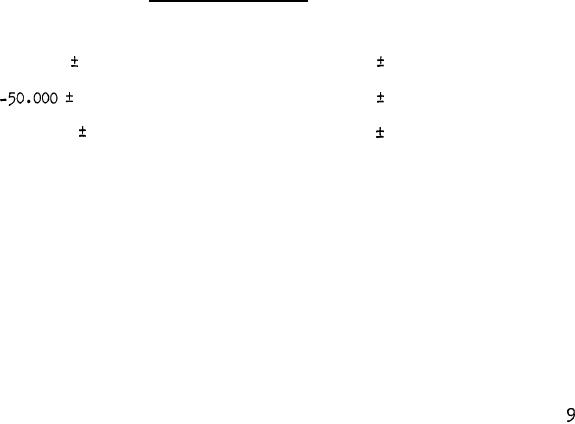
TABLE 5
DMma READOUT TIMES
Set-in Volts DC
Readout Seconds
0.020
-25.000
0.020 seconds
1.00
0.020
0.020 seconds
2.00
-100.000
0.020
0.020 seconds
4.00
3.3.11.3 T4 Output
3.3.11.3.1 Readout at 0.200 Volts. Elapsed time from the instant
a 0.200 voltage is applied in (c.) below until the voltage across pins D (+)
and W (-) of P3 reaches 4.0 plus or minus 0.5 volts DC, shall be as shown in
Table 6 after the application of voltages in the sequence specified in steps
(a. ) through (c.). The variation of plus voltage between pins D (+) and W (-)
of P3 shall not exceed 0.500 volts peak after application of the 100 milli-
second pulse in step (c.) and prior to completion of the time periods specified
in Table 6.
|
|
Privacy Statement - Press Release - Copyright Information. - Contact Us |
