 |
|||
|
|
|||
| ||||||||||
|
|  MIL-I-48331A(AR)
Input requirements. The microcircuit shall be
4.5.13.1
connected as shown in figure 5. The waveforms defined in
figure 6 shall be applied to the appropriate input terminals.
All input pulse magnitudes shall be equal to VDD except
onterminal 4. The voltage levels applied to input terminal 4
during the sequence test must be the maximum and minimum LVD
voltages specified in Table II for all values of supply
voltages (VDD).
4.5.13.2 Input clock characteristics. All pulse counts
shall be referenced to the zero start time. One pulse count is
equal to one pulse of the oscillator (terminals 1-2) and shall
conform to the characteristics defined in paragraph 3.3.5.
Input terminal number four (4) LVD
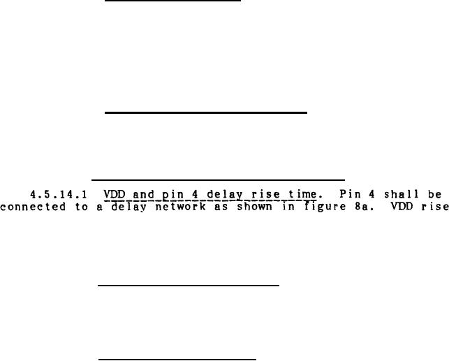
4.5.14
time shall be set for one millisecond for all tests and
sequential operation tests except long SD time test. A VDD
rise time of 500 milliseconds shall be used for the long SD
time test.
4.5.14.2 VDD and pin 4 rise time. Pin 4 shall be
connected to VDD directly as shown in figure 8b. VDD rise time
shall be set for one millisecond for all-tests and sequential
operation tests except long SD time test. A VDD rise time of
500 milliseconds shall be used for the long SD time test.
4.5.14.3 LVD function voltage: (terminal 15). The
microcircuit shall be connected to VDD directly as shown in
figure 13. A supply voltage (VDD) equal to 4.2 volts with a
rise time of 1 millisecond shall be applied to terminal 16. A
signal generator shall input 176 pulses as defined in 3.3.6 to
terminal 2 to initialize the circuit. The voltage on terminals
4 and 16 shall be decreased at a convenient rate while the
output voltage at terminal 15 is continuously monitored. When
a voltage transition from low to high occurs at terminal 15,
the magnitude of the supply voltage shall be measured as the
LVD voltage and shall conform to the requirements of Table II.
21
|
|
Privacy Statement - Press Release - Copyright Information. - Contact Us |
