 |
|||
|
Page Title:
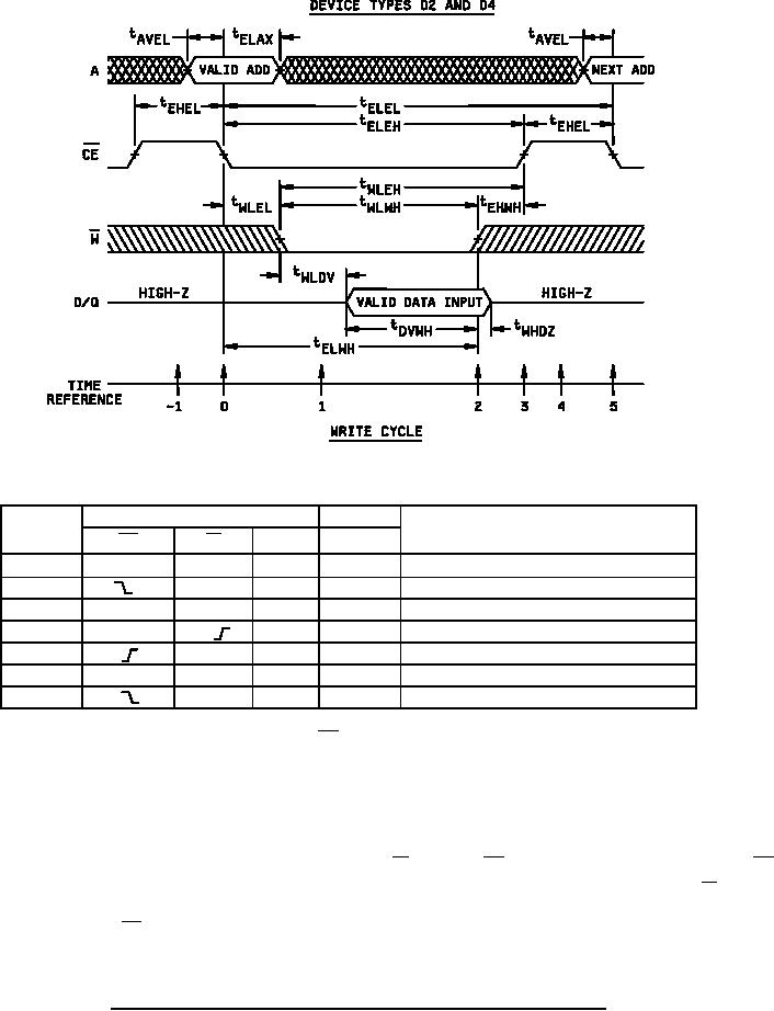
Figure 4. Read cycle, write cycle, read/modify/write cycle waveforms and truth tables Device types 02 and 04-cont. |
|
||
| ||||||||||
|
|  MIL-M-38510/245B
TRUTH TABLE
Inputs
Data I/O
Function
Time
reference
A
DQ
W
CE
H
X
-1
X
Z
Memory disable
0
X
V
Z
Cycle begins, addresses are latched
1
L
L
X
Z
Write period begins
2
L
X
V
Data in is written
3
H
X
Z
Write completed
4
H
X
X
Z
Prepare for next cycle (same as -1)
5
H
V
Z
Cycle ends, next cycle begins (same as 0)
The write cycle is initiated on the falling edge of CE (T = 0), which latches the address information in on chip registers.
If a dedicated write cycle is to be performed and the outputs are not to become active, tWLEL and tEHWH must be met.
Under these conditions, tWLDV is unnecessary and input data may be applied at any convenient time as long as tDVWH is
still met. If tWLEL is not met, then the outputs may become enabled momentarily near the beginning of the cycle and a
disable time (tELQZ) must be met before the input data is applied (tWLQZ = tWLDV). Similiarly, if tEHWH is not met the outputs
may enable briefly near the end of the cycle.
The write operation is terminated by the first rising edge of W (T = 2) or CE (T = 3). After the minimum required CE
high time (tEHEL), the next cycle may begin. If a series of consecutive write cycles are to be performed, the W line may
be held low until all desired location have been written. In this case, data setup and hold times must be referenced to
the rising edge of CE .
NOTE: See figure 5 for test conditions.
FIGURE 4. Read cycle, write cycle, read/modify/write cycle waveforms and truth tables - Continued
21
|
|
Privacy Statement - Press Release - Copyright Information. - Contact Us |