 |
|||
|
Page Title:
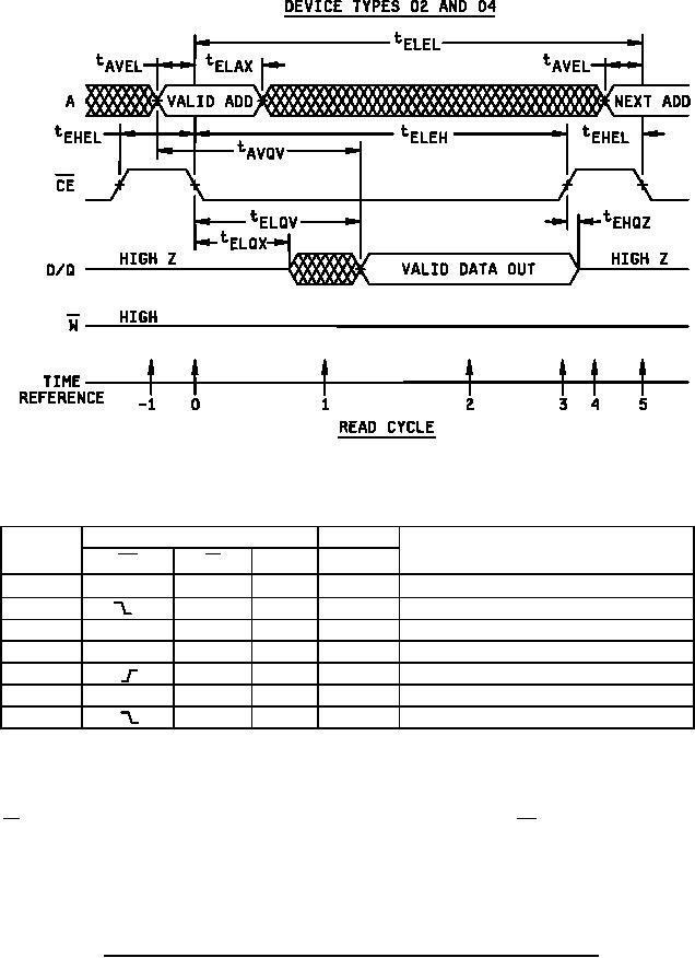
Figure 4. Read cycle, write cycle, read/modify/write cycle waveforms and truth tables Device types 02 and 04 |
|
||
| ||||||||||
|
|  MIL-M-38510/245B
TRUTH TABLE
Inputs
Data I/O
Time
Function
reference
A
DQ
W
CE
H
X
X
Z
Memory disable
-1
0
H
V
Z
Cycle begins, addresses are latched
1
L
H
X
X
Output enabled
2
L
H
X
V
Output valid
3
H
X
V
Read accomplished
4
H
X
X
Z
Prepare for next cycle (same as -1)
5
H
V
Z
Cycle ends, next cycle begins (same as 0)
The address information is latched in on the chip registers on the falling edge of CE (T = 0). Minimum address setup
and hold time requirements must be met. After the required hold time, the addresses may change state without
affecting device operation. During time (T = 1), the outputs become enabled but data is not valid until time (T = 2).
W must remain high throughout the read cycle. After the data has been read, CE may return high (T = 3). This will
force the output buffers into a high impedance mode at time (T = 4). The memory is now ready for the next cycle.
NOTE: See figure 5 for test conditions.
FIGURE 4. Read cycle, write cycle, read/modify/write cycle wave forms and truth tables Continued.
20
|
|
Privacy Statement - Press Release - Copyright Information. - Contact Us |
