 |
|||
|
Page Title:
Figure 5. Synchronous switching test circuit for device type 01. |
|
||
| ||||||||||
|
| 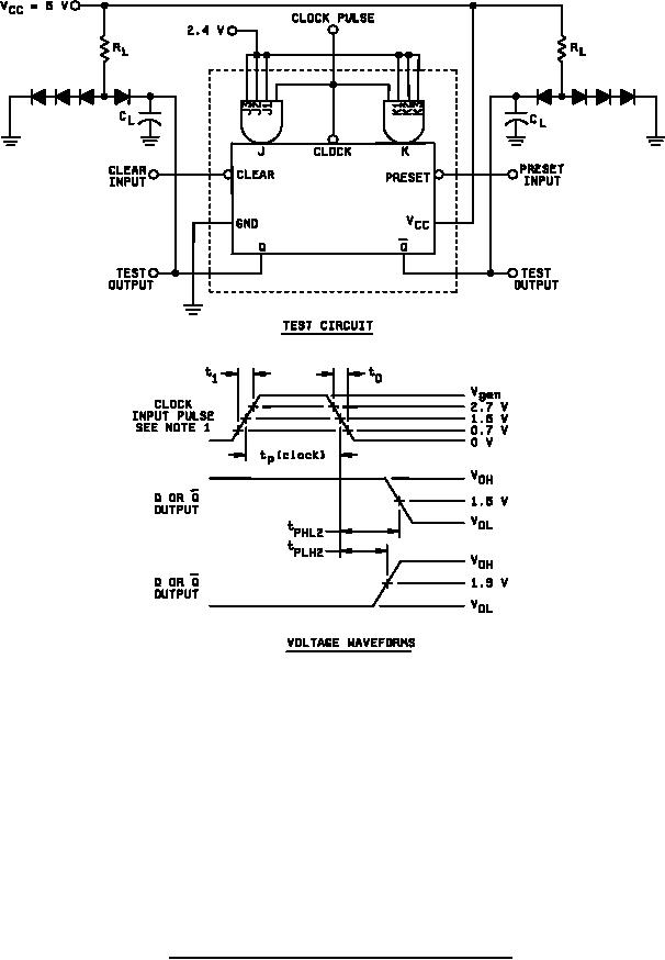 MIL-M-38510/2G
NOTES:
1. Clock input characteristics for tPLH, tPHL (clock to output), Vgen = 3 V, t1 = t0 ≤ 10 ns, tp (clock)
= 25 ns, and PRR = 1 MHz. All J and K inputs are at 2.4 V. When testing fMAX the clock
input characteristics are Vgen = 3 V, t1 = t0 ≤ 10 ns, tp (clock) = 20 ns, and PRR = see table
III.
2. J = J1 J2 J3; and K = K1 K2 K3
3. All diodes are 1N3064, or equivalent.
4. CL = 50 pF minimum (CL includes probe and jig capacitance).
5. RL = 390Ω 5%
FIGURE 5. Synchronous switching test circuit for device type 01.
24
|
|
Privacy Statement - Press Release - Copyright Information. - Contact Us |
