 |
|||
|
Page Title:
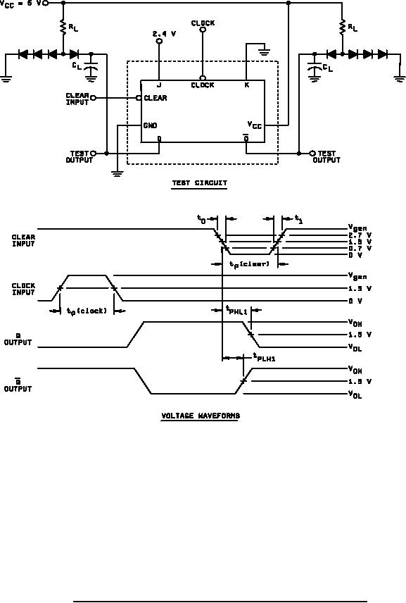
Figure 6. Clear switching test circuit and waveforms for device types 02 and 03. |
|
||
| ||||||||||
|
|  MIL-M-38510/2G
NOTES:
1. Clear inputs dominate regardless of the state of clock or J-K inputs.
2. Clear input pulse characteristics: Vgen = 3 V, t0 = t1 = 10 ns, tp(clear) = 30 ns, PRR = 1 MHz.
3. All diodes are 1N3064, or equivalent.
4. CL = 50 pF, minimum (CL includes probe and jig capacitance).
5. RL = 390Ω 5%.
6. Clock input pulse characteristics: Vgen = 3 V, tp (clock) ≥ 25 ns, PRR = 1 MHz.
FIGURE 6. Clear switching test circuit and waveforms for device types 02 and 03.
25
|
|
Privacy Statement - Press Release - Copyright Information. - Contact Us |
