 |
|||
|
Page Title:
Figure 4. Read cycle, write cycle, read/modify/write cycle waveforms and truth tables Device types 01 and 03 |
|
||
| ||||||||||
|
| 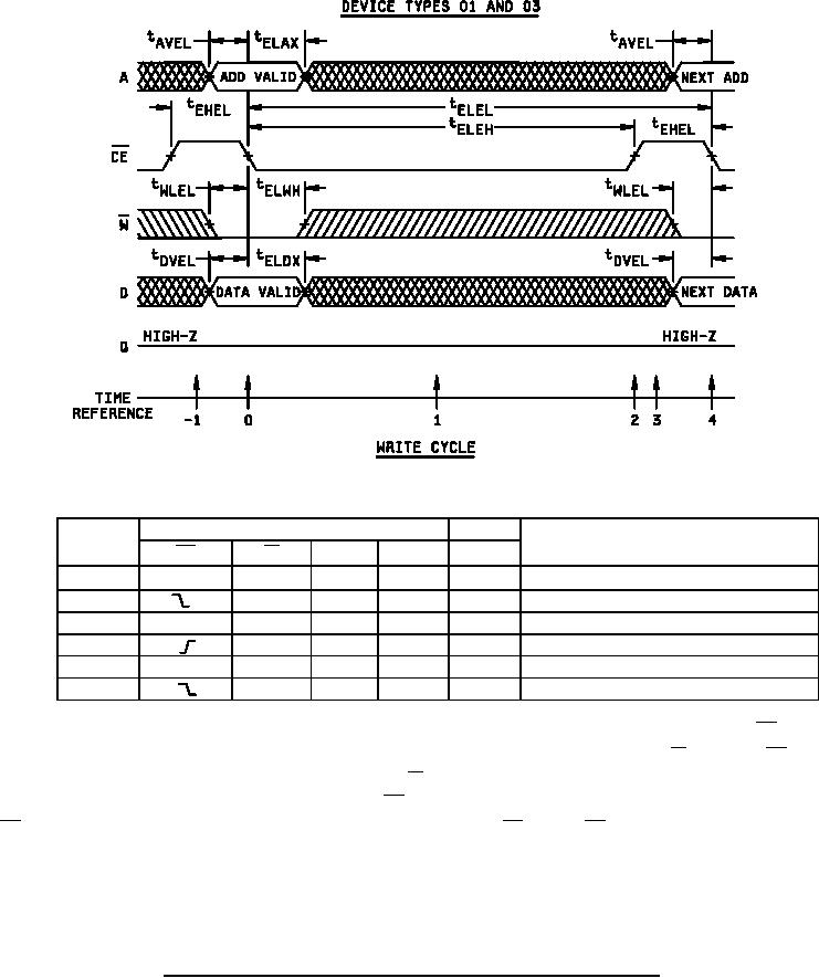 MIL-M-38510/245B
TRUTH TABLE
Inputs
Output
Time
Function
reference
A
D
Q
W
CE
H
X
-1
X
X
Z
Memory disable
0
L
V
V
Z
Cycle begins, addresses are latched
1
L
X
X
X
Z
Write in progress internally
2
X
X
X
Z
Write completed
3
H
X
X
X
Z
Prepare for next cycle (same as -1)
4
L
V
V
Z
Cycle ends, next cycle begins (same as 0)
The early write cycle is the only cycle where the output is guaranteed not to become active. On the falling edge of CE (T = 0),
the addresses, the write signal, and the data input are latched in on chip registers. The logic value of W at the time CE falls
determines the state of the output buffer for that cycle. Since W is low in the early write cycle, the output buffer is latched into
the high impedance state and will remain in the state until CE returns high (T = 2). For this cycle, the data input is latched by
CE going low; therefore data set up and hold times should be referenced to CE . When CE (T = 2) returns to the high state, the
output buffer disables and signals are unlatched. The device is now ready for the next cycle.
NOTE: See figure 5 for test conditions.
FIGURE 4. Read cycle, write cycle, read/modify/write cycle waveforms and truth tables Continued.
18
|
|
Privacy Statement - Press Release - Copyright Information. - Contact Us |
