 |
|||
|
Page Title:
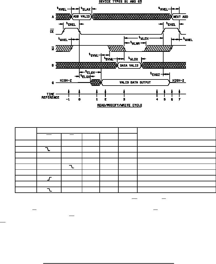
Figure 4. Read cycle, write cycle, read/modify/write cycle waveforms and truth tables Device types 01 and 03-cont. |
|
||
| ||||||||||
|
|  MIL-M-38510/245B
TRUTH TABLE
Inputs
Output
Time
Function
reference
A
D
Q
W
CE
H
X
X
X
Z
Memory disable
-1
0
H
V
X
Z
Cycle begins, addresses are latched
1
L
H
X
X
X
Output enabled
2
L
H
X
X
V
Output valid, read and modify time
3
L
X
V
V
Write begins, data is latched
4
L
X
X
X
V
Write in progress internally
5
X
X
X
V
Write completed
6
H
X
X
X
Z
Prepare for next cycle (same as -1)
7
H
V
X
Z
Cycle ends, next cycle begins (same as 0)
The read/modify/write cycle begins as all other cycles on the falling edge of CE (T = 0). The W line should be high at (T = 0)
in order to latch the output buffers in the active state. During (T = 1) the output will be active but not valid until (T = 2). On the
falling edge of the W (T = 3), the data present at the output and input are latched. The W signal also latches itself on its' low
going edge. All input signals excluding CE have been latched and have no further effect on the SRAM. The rising edge of
CE (T = 5) completes the write portion of the cycle and unlatches all inputs and the output. The output goes to a high
impedance and the SRAM is ready for the next cycle.
NOTE: See figure 5 for test conditions.
FIGURE 4. Read cycle, write cycle, read/modify/write cycle waveforms and truth tables Continued.
19
|
|
Privacy Statement - Press Release - Copyright Information. - Contact Us |
